[Industry] Semiconductor-3: Manufacturing Process
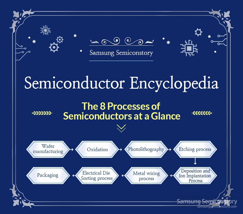
Wafer Preparation:
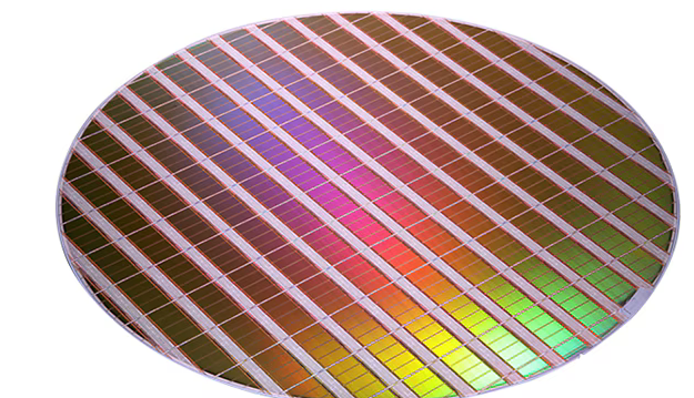
Extracting Silicons => Purification => monocrystalline ingots => Slicing & Grinding =>...
=> Substrate for microelectronic devices
Oxidation:
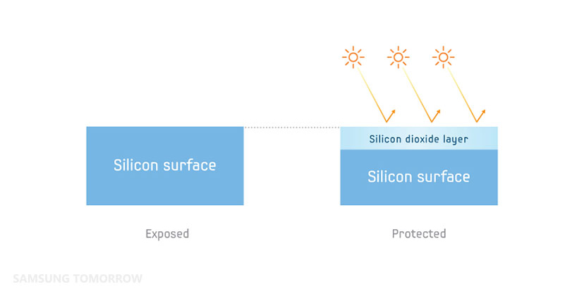
Create a 'Glass Layer’ to block current flow and entry of other substances.
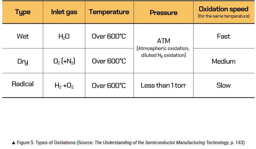
Si+O₂→SiO₂: Dry Oxidation, Slow (∵ O2 > H2O ), High quality
Si + 2H2O → SiO2 + 2H2 :Wet Oxidation, Fast/Low quality
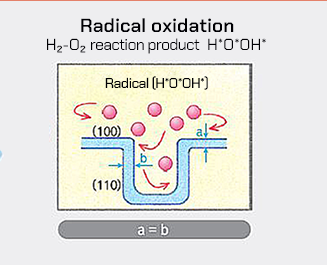
Radical Oxidation: Slow, Best quality as using ‘Highly reactive gas’
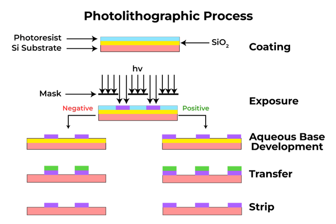
Photolithography:
PR Coating to wafer => Ultraviolet light passes through a mask/reticle => A certain pattern applied on surface
Etching:
Removing material to form circuit features:
Wet Etching: Uses liquid chemicals (e.g., hydrofluoric acid) for isotropic removal
Dry Etching: Employs plasma (e.g., reactive ion etching/RIE) for anisotropic, high-precision patterns.
Deposition:
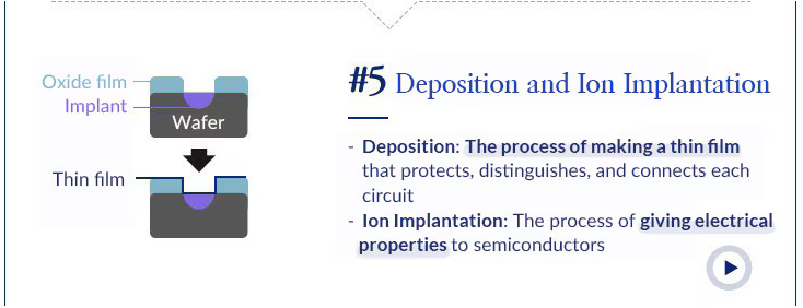
Deposition might be applied ‘before’ photolithography if necessary
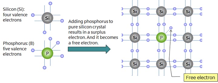
Doping:
Giving silicon abundant "free" electrons (or holes) that are weakly bound and easily move under a weak voltage,
boosting conduction without collapsing the precise crystal structure.


Comments
Post a Comment